The printed circuit board (PCB) is a core component in most electronic devices, where its role is to connect electrical components onto itself in a way that facilitates complex electronic interactions. However, it is very hard to take off. While these circuits are vulnerable to electromagnetic interference (EMI), which can be detrimental to their performance and reliability, they offer certain advantages, including being resilient against harsh environmental conditions and easy replaceability. The avoidance of usable electric circuits against EMI shielding cans is, hence, important for the operation of a wide range of applications. In this article, designing effective PCB shielding is discussed, and the benefits of each method are discussed.
Understanding Electromagnetic Interference (EMI) of PCB shielding
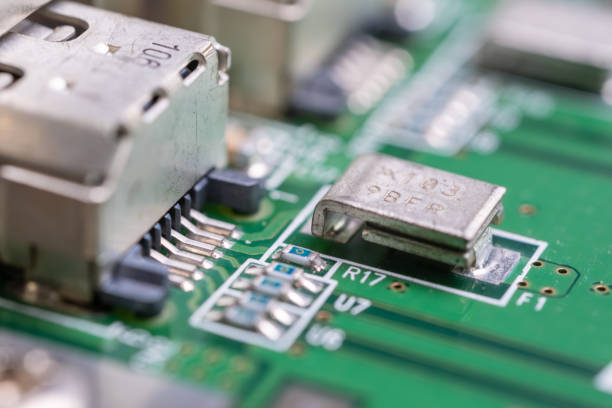
Before discussing protective techniques against EMI, it’s worthwhile to understand EMI itself and why it’s regarded as an issue. EMI, or electromagnetic interference, refers to a disturbance caused by an external disruption that can affect an electronic circuit using electromagnetic induction, electric coupling, electromagnetic radiation or conduction. Interference in the electromagnetic energy form can result from different sources, such as radio waves, electric motors, radio frequency interference and other electronic equipment.
Types of PCB Shielding
Here’s a brief overview of the different types of PCB shielding techniques:
Material Shielding: Employs a variety of materials like metal shielding cans or conductive foams, which represent EMI-blocking or EMI-absorbing types.
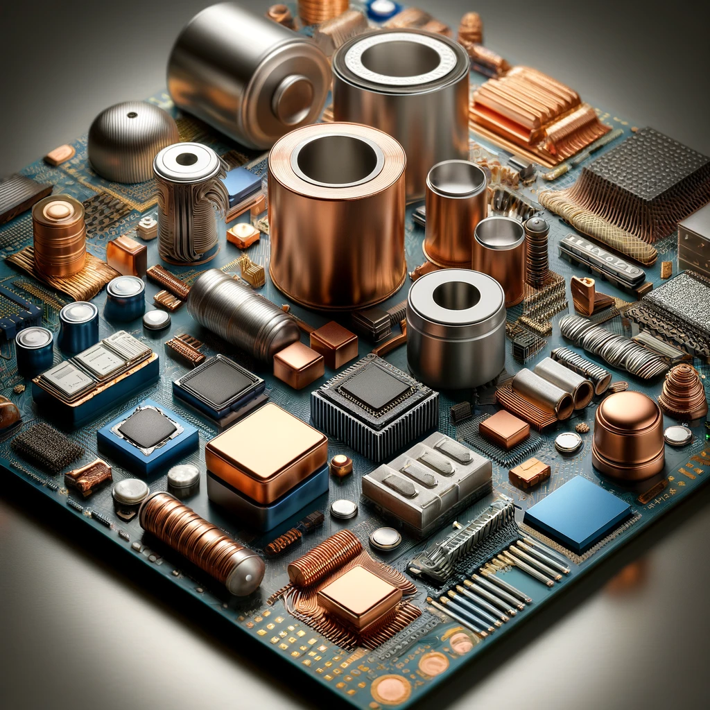
PCB Layout Optimization: Embedment by utilizing strategic trace routing and impedance control techniques for reduction of EMI susceptibility.
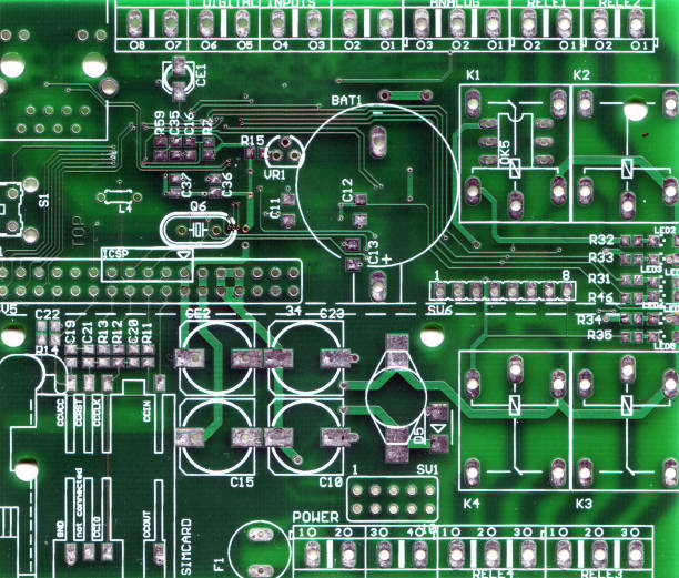
Shielding Cans: PCB boards with casings in metal soldering to cover up the various types of components so as to provide protection from Faraday effects.
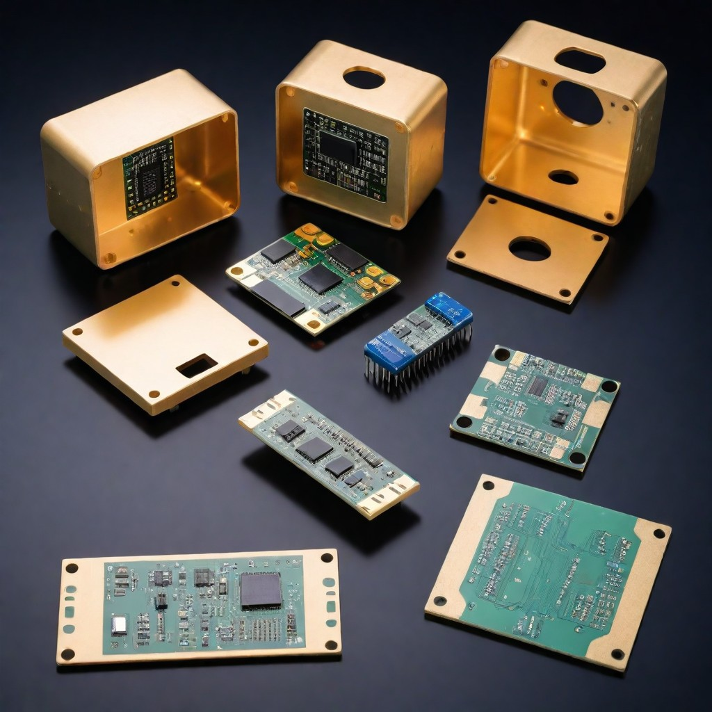
Conductive Coatings: Materials, e.g., conductive paints or coatings, are applied to the PCB in order to provide electromagnetic shielding.
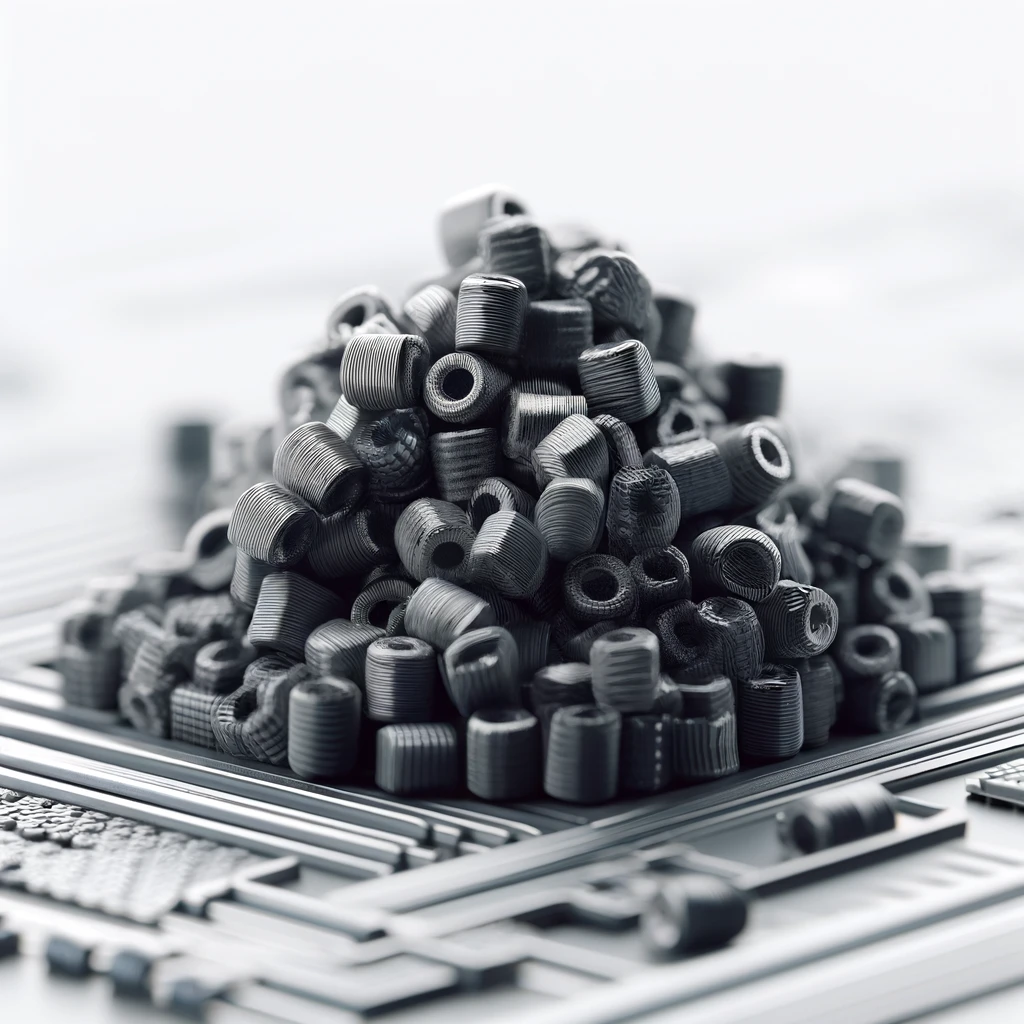
Ferrite Beads: Ferrite cores are used to filter out radio-type interference by attaching them to any wire or cable.
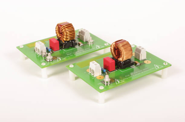
EMI Filters: The components of the PCB are designed so as to engage interference cancellation of undesired high-frequency noise and forward transmission of required frequencies.
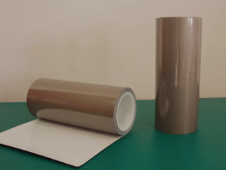
Shielding Films: Copper or aluminum conductive forms shall be used with PCB by applying thin layers at the circuit localized shielding.
Implementing EMI Shielding in Your PCB Layout
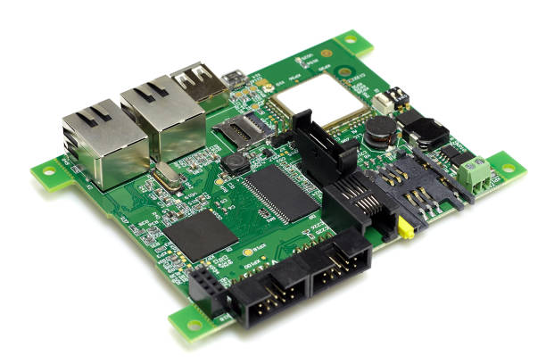
Implementing EMI shielding effectively in your PCB layout involves several strategic steps:
- Material Choice: Choose materials that manage electromagnetic wave emc shielding in an excellent way for PCB layers and enclosures.
- Component Placement: Strategically site sensitive electronic device at a safe distance from EMC sources yet close to ground plane.
- Trace Routing: Design high-speed net and routing traces away from the noise area where possible and keep them short in length.
- Grounding: Develop in-depth and broad-based earthing technology for the crew members. Multiple ground layers, if it is practicable, could be used so that the protection is like layers of tissues.
- Shielding Cans:Putting the sensitive electronic circuits and cans of metal on top of the particularly noisy circuits can make the circuit interior noisy for EMI.
- Conductive Coatings: Cover the areas where no electronic components are visible at this stage with conductive paint or paint spray so as to provide the expected level of protection from EMI.
- Ferrite Beads: Add ferrite beads to power supply lines and signals, which will be effective in suppressing high-frequency noise.
- Decoupling Capacitors: Arrange these capacitors side by side on the pin-voltage pins of active components.
- Guard Traces: source shortening vias made of guards to ground to protect lines with high frequencies or sensitive ones against interference or high conductivity mesh materials.
- Differential Signaling: Couple lines instead of installing single lines in order to reduce their presence in signal transmission.
Shielding at the Lowest Possible Levels
To effectively implement EMI shielding at the lowest possible levels in PCB design, consider the following strategies:
- Use Shielding Materials: Utilize the PCB designers substrates and conductive layers, which provide the shielding features that facilitate the attenuation.
- Shield Sensitive Components: Align small shielding cans or covers directly with the most vulnerable ones.
- Optimize PCB Layout: Attempt for the direction of sources and paths of EMI to be done in a way that its overall level will be minimized. For example, place voltage elements away from the high-frequency component.
- Enhance Grounding: The primary grounding strategy should be implemented with complex grounding services utilizing several ground wires and connections.
- Apply Conductive Coatings: Acquire conductive paints or films and put them on the PCB to ensure the double barrier for EMI prevails.
- Integrate Ferrite Beads: Install ferrite beads on cables and near connectors to dampen the high-frequency noise if volumetric interference is still present.
- Use Differential Pairing: encode signals as differential pairs for the woman, resulting in a primary reduction in EM radiation exposure.
- Decoupling and Filtering: Install decoupling capacitors at the output and add the filters to the lines that carry power. This will allow us to prepare the power and address EMI issues.
Traditional PCB Shielding Techniques
The variety of electromagnetic interference (EMI) shielding tricks in traditional PCBs are essential for reducing the level of EMI and guaranteeing the normal functionality of electronic circuits. Here’s an overview:
- Ground Planes: An abundant amount of ground planes is responsible for shielding signal lines, thus cutting down the vulnerability to EMI at the same time.
- Shielding Cans: One of the most commonly used shielding elements is the metal cans, made out of cardboard or plastic, which is used to cover the components or circuits with the sole purpose of protecting them from receiving various electromagnetic interferences.
- Conductive Coatings: Conduction paints make this possible via an application process to the PCB, where the conduction layer shields the board from EMI.
- Trace Routing: Attentive routing of the traces to confine their exposition towards likely EMI sources and to have minimal loop areas that are susceptible to interference.
- Ferrite Beads: They are found on the circuit PCB entering the cables and are used to turn off or eliminate high-frequency noise that is travelling through the circuit.
- EMI Filters: Filters are dime a dozen, but the manufacturers need to consider providing filters that will better manage unwanted high-frequency electromagnetic pollution and pass the required frequencies.
- Copper Foil: The copper foil insertion at particular locations of the PCB shall help to form the shielding; this approach is particularly useful for some quick fixes and prototyping.
- Chassis Grounding: Connecting the PCB to the metal chassis of equipment can make the chassis an extra shielding mechanism that protects EMI while at the same time increasing shielding.
PCB shielding can, example pictures
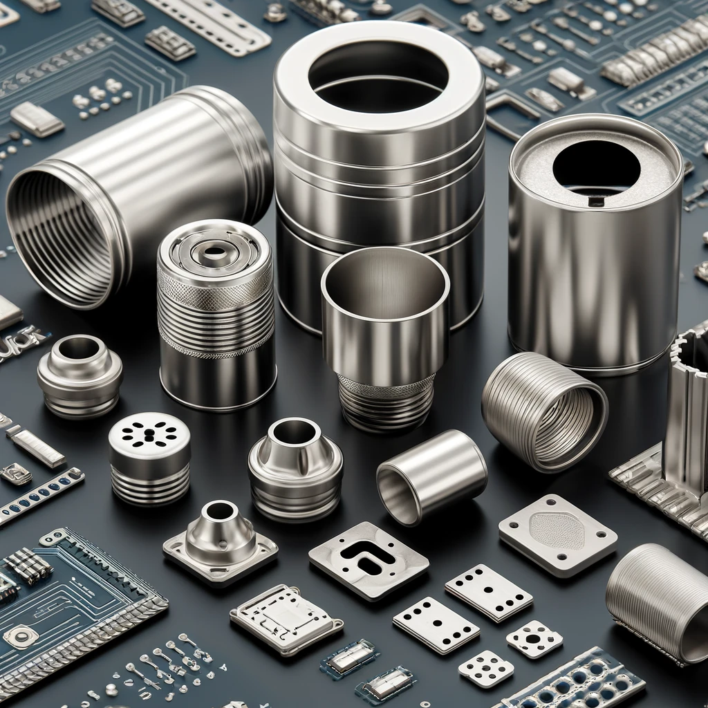
The next series of images will highlight different types of protective materials that can work inside the PCB shielding. Each image highlights a specific material: nickel-silver, aluminum, or tin-plated steel. The composition and design ideas play off their individual features. These are utilized to soften out the surroundings for sensitive elements on a PCB.
Let’s take a look at this illustration that exhibits the diverse PCB shielding can design that includes nickel-silver, aluminum, and tin-plated steel cans. Each of them is intended to be mounted over certain areas of a PCB to keep EMI from harming the internal parts.
Enclosure-Level EMI Shielding Techniques
Enclosure-level EMI shielding concentrates on the electromagnetic coupling immunity, which prevents interference via the electronics devices that are installed within a certain enclosure. The precision of these techniques is essential so that the devices function normally without external electromagnetic sources’ disruptions. Use our AI to write for you about any assigned topic. Here are several common enclosure-level EMI shielding methods:
- Conductive Coatings: First, electrodes can be made from metals like nickel, copper, and silver, to which conduct paints can be applied to sculpt the shape of the enclosure of the electrode inside. Through the application of this coating, the processes develop a conductive layer; therefore, the devices are protected from EMI.
- Metal Enclosures: The enclosure’s construction is an important factor. I will utilize materials that tend to naturally block EMI. These metals include aluminum or steel, which are conductive. This is one of the key methods of blocking different wavelengths of influencing radiation.
- EMI Gaskets: Putting in gaskets to avoid EMI spill is helpful for the sealing up of the enclosure. These gaskets are made from conductive materials like metal-filled silicones or woven mesh meshing which enhances the conductivity properties between two adjacent conductors.
- Shielded Cables and Connectors: Creating special cables that are designed to eliminate EMI, by such means as shields and short cables. They are commonly surrounded by metal shieldings that are either braided or foil components.
- Ventilation Panels: Utilizing the conductive mesh or metal perforated panel ventilation other electronic systems that provide air flow while EMI is being blocked.
- Absorbing Materials: The solution here is to fill the enclosure with the materials that to slight the electromagnetic radiations. These possibilities refer to such things as polyurethane foam or other ferrite material.
- Board-Level Shielding Inside the Enclosure: Implementing an enhanced shielding at the PCB side, by means of shield cans, or a conductive paint, or another layer of shielding would be an effective method of minimizing RF interference.
Effects of EMI on PCBs
It is one of the many kinds of electromagnetic interference, which in fact severely affects the functionality and performance level of printed circuit boards (PCBs). Here are some of the primary effects EMI can have on PCBs:
- Signal Disruption: EMI results in noise that tends to spoil the signals on the PCB thus, causing errors that could lead to malfunction of the PCB.
- Data Corruption: In information technology, EMI will cause data breaches or malfunction.
- Reduced Performance: Noise that affects EMI as a result can be harmful to work efficiently and achieve the objectives set.
Techniques for Shielding PCBs
Shielding printed circuit boards (PCBs) from EMI involves using a lot of methods that are aimed at the protection of electronic gadgets from interference of external or internal electromagnetic field variations. Here are some effective methods for shielding PCBs:
1. Material Selection
The basic approach remains the same of using materials that by nature are capable of reflection and protection of electromagnetic waves. In addition the materials like mu-metal, a nickel-iron alloy, are believed to have perfect magnetic permeability, which results them in high magnetic shielding.
2. PCB Layout Optimization
- Trace Routing: Keep the length of the high-speed traces less to ensure that they are not so close to possible sources of interference.
- Grounding: Adopt an elaborate shunting entire system for enveloping the shield against EMI. The presence of many grounding points may be one of the means to increase the loop surface area, which results in the initial emissions reduction.
3. Shielding Cans
Solder connectors may be attached directly onto a PCB soldered to sensitive areas or circuit loops. These cans introduce Faraday cages roles, actually protect an occupied area from any external electromagnetic (EM) waves.
4. Conductive Coatings
EMI can be shed to the non-interfering part of the PCB when a conductive paint or coating is applied to the PCB. These coatings are machines which are made out of nickel, silver or copper for instance.
5. Ferrite Beads
Ferrite beads can be placed on power conductors incoming side to eliminate electromagnetic interference. They operate by attenuating the high-frequency effects, which impede transmission through the circuit altogether.
Benefits of Effective PCB Shielding
An excellent shielding in the PCB can be seen in the electronics devices that many benefits envisage and promotes good functioning and lifespan of the devices. Here are some of the key advantages:
Improved Reliability
The presence of shielding reduces the chance that an EMI-induced failure may occur, consequently it ensures devices work in every one of those electromagnetic environments reliably.
Enhanced Performance
EMI mitigation by shielding technologies supports efficient functioning of digital devices under the severed circumstances. Furthermore, the performance standard of electronic devices is maintained in diverse conditions.
Compliance with Standards
One of the significant challenges that manufacturers of electronic devices such as smartphones, computers, and radio equipment face the world over are their compliance to international electromagnetic compatibility (EMC) standards. Shielding for the materials provides the Write a statement that promotes to encourage recycling among students.
Standard shielding cans, part numbers ( length, width and height)
PCB shielding cans applied for standard cases, designation of codes is describing of their dimensions( length, width and height). For example, the Holland Shielding energy Systems provide different size can protectors of 1500 and 1510 series. They have hidden codes that follow a specific numerical pattern in their product names. Such numerical sizes always express dimension in millimeter, for example, length, width, and height.
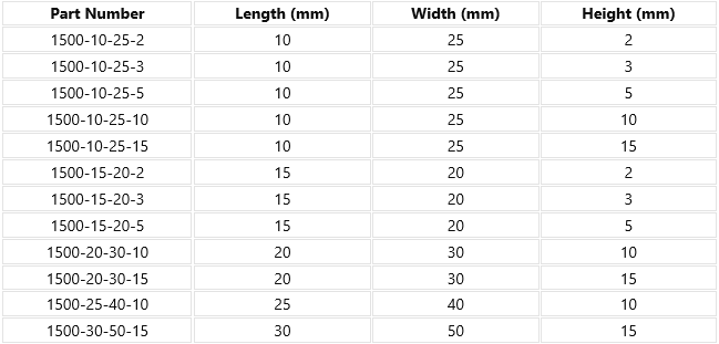
For instance:
- The part identifier – 1500-10-25 -5 you can find the can for gathering a spectrum with the length equal to 10 mm, width equal to 25 mm, and height equal to 5 mm.
- Here is another instance of a code, 1510-20-20-10, signifying a length of 20 mm, a width of 20 mm, and a height of 10 mm.
Here is factors assist in choosing the can that fit for the specific size of the PCB being shielded. The electrode numbers and dimensions can vary quite a lot when it comes to producing different applications and PCBs of different sizes. Often, custom sizes can be manufactured upon request (as long as these are produced cost-effectively).
Rectangular PCB shielding cans ( length, width and height)
Square PCB shielding cans being the components, these are used on the electronics to protect delicate circuits against the electromagnetic interference. The metal can of such capacitors is also a conductor and covers certain critical areas on a printed circuit board (PCB) where sensitive components are situated.
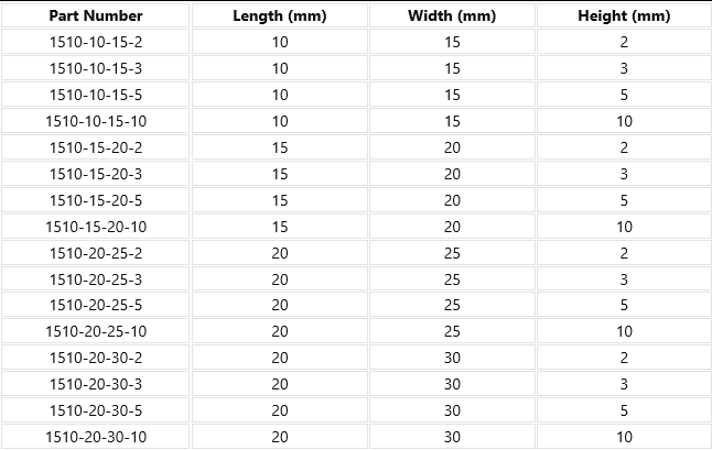
The exact dimensions of those screens, which are length, width, and height, are crucial; they must only cover the components they are intended to protect, while at the same time being able to fit without interfering with other parts of the PCB. The dimensions of length and width give the footprint of the can on the card, but for the box parts to fit there is also a need for a height, which corresponds with the need for vertical space.
As an example, using a typical case, which would have the part number 1510-10-15-10, the dimensions could be 10 mm long, 15 mm wide and 10 mm high. The measurements allow the case to accommodate the components while maintaining a low profile with a view of fitting seamlessly within the assembly of the device.
What are elastomer electromagnetic shielding materials?
Elastomer electromagnetic shielding materials is a type of electromagnetic interference which is shaped as a conductive composite applied for documentation of EM (electromagnetic) to halt or at-least reduce interference. This material is described as conductive filler blends, like metal particles, carbon black or graphite which are added in to a rubber base to get it. There are main components in the implant, they are biocompatible material, the shell and the filling. Usually, the base material is a flexible polymer, such as silicone, rubber, or a thermoplastic elastomer.
- Flexibility: In contrast to inflexible shielding solutions, elastomers have flexibility property which provides them advantage to be used in applications where seals or gaskets can shape to non-uniform surfaces or shapes.
- Conductivity: The charged particles in the elastomeric polymer make a way forming the path where charge can get rid of or be reflected to prevent the EMC. It is notably an important factor in effective EMI barrier.
- Environmental Resistance: Often these compounds, along with carbon fiber and steel, which provide excellent properties of resistance to extreme temperatures, UV radiation, and chemicals, are commonly used for applications that need to endure harsh conditions.
- Customizability: The nature of the shielding material can be modified by changing the type and amount of particles what is in the material mixture (filler). This made for personalized fits for the ship’s hull, so that the specific shielding effectiveness requirements could be achieved.
- Ease of Installation: Two-piece elastomer seals can be molded into different forms, such as panels, gaskets or O-rings, and these seal parts can be easily installed on complex assemblies.
The elastomer EMI shielding products are quite applicable and can be found in the space, automotive, electronics and telecommunication industries. These materials can protect electronic equipment in high EMI environments and improve overall electronics performance.
Applications of Printed circuit board shielding
The print shield is usually employed for the purpose of controlled/limitation of electromagnetic and radio-frequency interferences such EMI and RFI. It is crucial not only for retaining the accuracy and efficiency of the electronic systems but also with the cases when the environment is electromagnetically busy. Here are some common applications:
- Medical Devices: PCB shielding is pivotal to all medical equipment so as to save the precise diagnostics and update the reliable performance in the systems like MRI machines and patient monitoring systems.
- Consumer Electronics: In components like smartphones, laptops, and televisions PCB shielding intervenes in devices malfunctioning that may compromise sensitive features and erode user experience performance.
- Automotive: Vehicle incorporation of electronic systems nearly for navigation, control, and entertainment, shielding of PCB is badly needed for blocking the interference coming from these systems and maintaining them work well under different electromagnetic circumstances.
- Military and Aerospace: In these environments, the high-reliability (faithfulness) and precision of inside electronic systems are paramount.PCB shielding techniques
Conclusion
The art of PCB shielding is not only about the way of implementing the necessary techniques, but also about the adverse effects the device will face in operation. Through using a variety of the materials, design modifications and inserting the additional shielding elements the designers are able to manufacture devices that will work well and avoid the disruption of the harmful electromagnetic waves. In this way, well-designed shielding can get over problems of reliability, ease of use, and improve the features of the electrical devices. It has an impact on their compliance and market success.

