The world of printed circuit board (PCB) production test means meeting an unwavering requirement for quality and reliability. As a means to this end, the flying probe testing technique stands out not only for its flexibility, accuracy, and efficiency but also because it is up-to-date and automates most of the tasks to test program. This article will give you an idea of the complexities surrounding flying probe testing, as well as the pros and cons of how it is fitted into the fabrication of printed circuit boards.
What is flying probe testing?
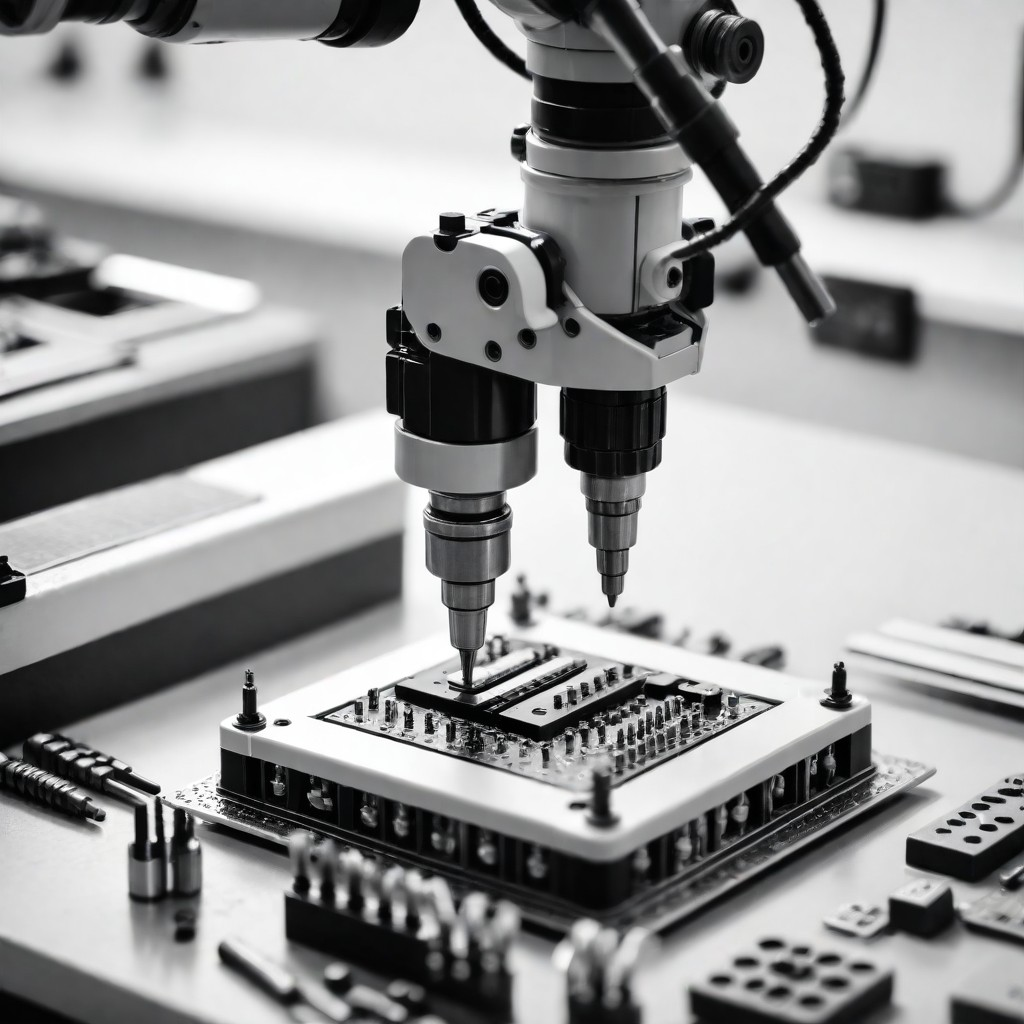
Flying probe testing is one of the sophisticated forms of electrical testing that is used specifically for printed circuit boards (PCBs). Unlike the traditional microroom needles under the nails testing setups that need to receive conduct, a flying pen storage tester draws a small number of the movable probes. For example, diagnostics like probes can be programmed to quickly advance to various locations on a PCB based on the based on the conductivity and functionality of components to the electrical test.
Types of Flying Probe Test Systems
Flying Probe Test systems could be grouped into some types by their capabilities and application areas to test programs. Here’s a brief overview of the common types:
Single-Sided Systems: Through the use of scratch probes that only touch one side of PCBs, these systems eliminate faulty traces. They are a good choice for generic boards with test points on one side and avoid populated boards with aluminum vias interfering on the other side to test point.
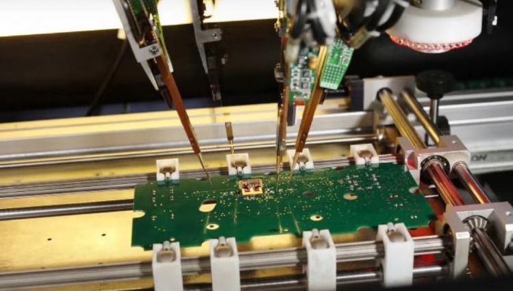
Double-Sided Systems: These testers are designed with probing tips that can give contact to both sides of the circuit board simultaneously. This feature empowers the testing of much more complicated boards that have components on both sides.
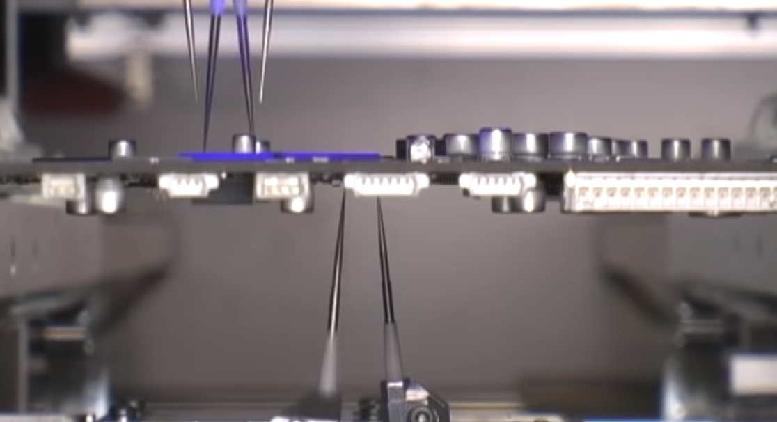
Multi-Probe Systems: Carrying out several tests at once, these systems employ several probes that help them to shorten their run times and better satisfy the demands of more complex and, in some cases, more volumetric ones.
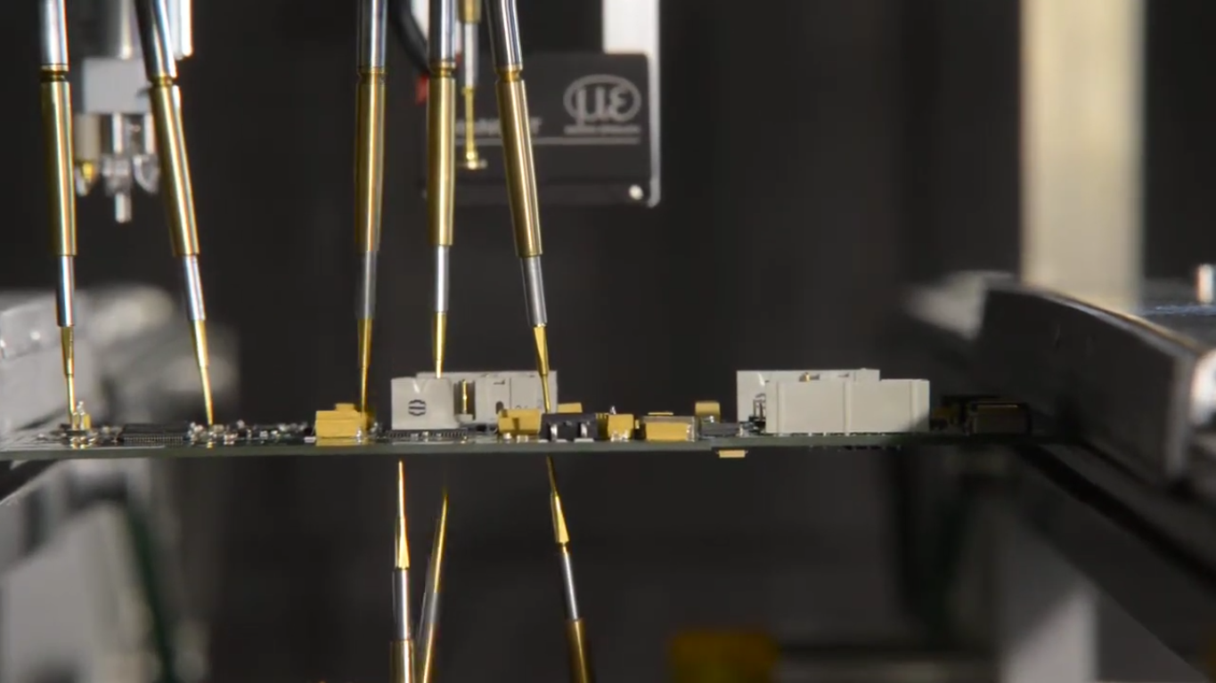
High-Speed Systems: Being compact and designed to test samples quickly, they are perfect for quickly cycling between tests, hence increasing throughput, which is the key to maintaining the smooth functioning of a high-volume production or some have mid volume production.
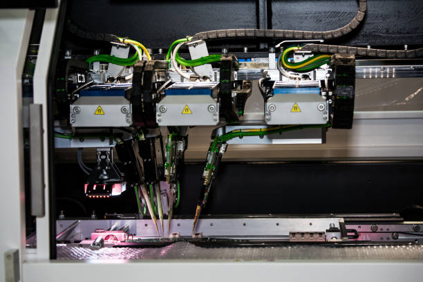
Grid Systems: Unlike typical systems, which use a testing grid that is fixed for layout, some other systems apply a probe grid that can be changed easily according to every pattern of a certain PCB, reducing the costs of reprogramming.
The system types are not very homogenous, but like with any testing system, there is some overlapping flying probe system. Each kind of system is better suited to address certain testing needs and complex environments in production.
There are several reasons for eventual adoption of the populated boards

The adoption of testing methods for populated PCBs is crucial for several reasons:
- Quality Assurance: The operator is responsible for placing, soldering, and checking that all components are in place and the board functions as expected.
- Fault Identification: Avoids the delay in detection and diagnosis of errors at the initial stage, thus saving time and money in rework.
- Component Verification: Identifies that the correct components are both authentic and specified in accordance with the required specifications, and that all the parts are functioning normally or otherwise.
- Reliability Testing: This simulation test checks for the board’s endurance across several scenarios, and this is what guarantees the long-term reliability of the prototypes.
- Compliance: It makes sure that the PCB is on par with some of the industry requirements and upholds the standards set by the regulatory authorities.
- Cost Efficiency: Averts costly financial recalls and builds customer loyalty by guaranteeing that products leave the supplier’s door in the right condition.
Boards populated with more sample boards are vital for preserving high standards of PCB manufacturing and guaranteeing the later success of the actual electrical schematics.
Flying probe test serves two critical purposes
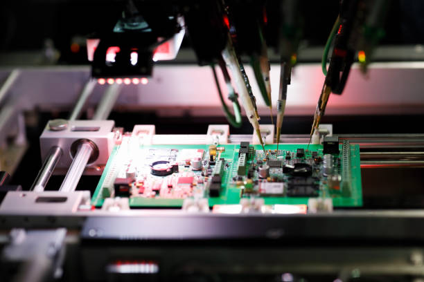
Flying probe testing primarily serves two critical purposes in PCB manufacturing to the flying probe test system:
- Defect Detection: Locate imperfections like connections, shorts, and components on the PCB during manufacturing.
- Functional Verification: Observes the satisfactory operation of components as well as the assembled board, so that the PCB operates as it is designed to.
Advantages of Flying Probe Testing
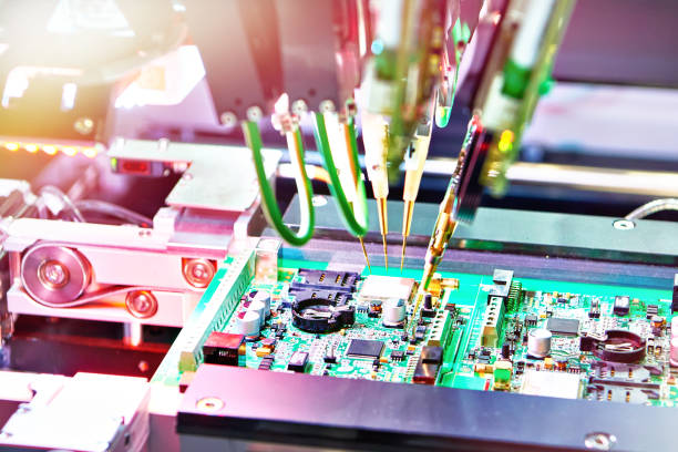
Here are the key advantages of flying probe testing:
- Flexibility: Allows for software revision without special fixtures and faster prototype preparation.
- Cost-effective: reduction in set-up costs if compared with conventional molding and flexible cost structure for small- to medium-volume manufacturing.
- Detailed Diagnostics: Gives diagnostic abilities that are more accurate and closer to the right location.
- No Physical Fixtures Required: It uses no test sensors or fixtures for approval, thus saving both money and time for preparation.
- Quick Setup: Accomplish quick and consistent changes across different designs of PCB.
- High Accessibility: Test compact PCBAs and small test points, which are inaccessible with conventional bed-of-nails testers.
- Non-Destructive: reduces the chance of PCB damage when it is tested, and by that, it outlines the level of product quality.
Disadvantages of Flying Probe Tests
Here are some key disadvantages of flying probe testing:
- Slower Testing Speed: In contrast to a bed-of-nails tester, a flying probe may take time; thereby, the more production there is, the slower it will be.
- Limited Throughput: Capable of producing only a small number of units since it is based on a single-directional testing principle.
- Higher Operational Costs: If it becomes a limitation because of the lower speed, it can incur higher costs per test in high-volume situations.
- Complex Programming: This involves customizing a set of codes or instructions for each new design.
- Mechanical Wear: Probes and parts in ruination are contributing to friction and need replacing or repair.
- Limited Test Coverage: This screening type cannot only detect but also distinguish between different types of insulation, like high-voltage insulation, as powerfully as other technologies.
How Flying Probe Testing Works
Flying probe testing works through the following key steps:
- Programming: The sequence of tests is programmed based on PCB design and the particular purpose in mind.
- Setup: The PCB is inserted into the autorouter while the probes are aligned to the diagnostic plan.
- Testing: Probes are mobile, so they can move into any test position on the PCB that is to undergo the electrical contact tests (connectedness and component function testing).
- Analysis: The machine records the test results after adding them to the system and detects any discrepancies or failures.
- Reporting: Resulting from the test outcomes, a detailed report is created, and the areas of deficiencies or problems found during that process are signaled in that report.
Applications of Flying Probe Testing
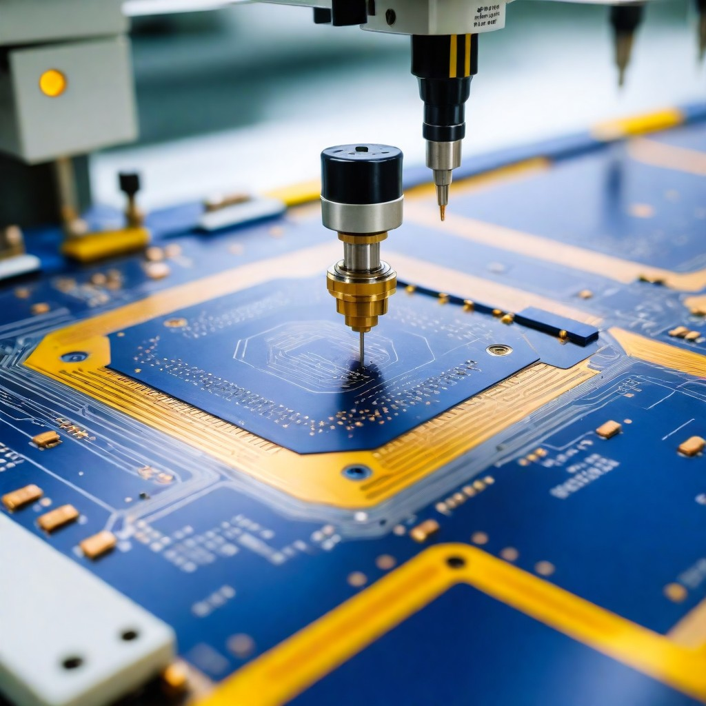
Flying probe testing is widely applied in several areas of PCB manufacturing.
- Prototyping cuts the production lead-time and cost of assembling dedicated provision machines and reduces the need for conventional soldering equipment.
- Low- to Medium-Volume Production: Distinctive when examining a small number of parts, such that a production line setup is more bulky and expensive.
- Complex Boards: Efficiently handles the analysis of exorbitantly complex PCBs that contain dense layouts and small components that cannot be reached easily by conventional methodology.
- Quality Control: Offers a high level of quality control and identifies early manifestations of defects in the components and sub-assemblies.
- Debugging: helpful in detecting problems and tracking their neat solution in the design phase.
- Repair Verification: Provides the other mechanics with confidence in their abilities by testing repairs after they are repaired.
Choosing the Right Flying Probe Tester
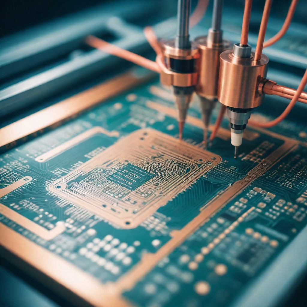
When selecting the right flying probe tester for PCB manufacturing, consider these key factors:
- Probe Count: Find out the exact number of probes you need based on the complexity and dimensions of the PCB you have.
- Speed: Include the timing requirements to meet your production deadlines in your practical considerations.
- Test Coverage: Evaluate the kind of testing machine it is and be sure that it fulfills all your testing needs.
- Accuracy: Guarantee that the tester gives both excellent accuracy of probe placement as well as test results.
- Flexibility: Seek for versatile solution which provides possibility for testing various kinds of designed PCBs.
- Software Interface: An advisable choice is to consider using a tester that has a user-friendly interface made to make it easy to program and do data analytics.
- Support and Maintenance: Also, one of the factors you need to look at are technical support and ease of maintenance.
- Cost: Estimate the cost-benefit analysis taking into consideration the required volumes of production, specific testing needs and long-term sustainability of operations.
Step by steps operations
Here’s a short step-by-step guide for performing a flying probe test on printed circuit boards (PCBs):
- Setup: Place the PCB on the test fixture and secure it properly to reduce shaking.
- Configuration:Type in the specification data as well as the design and test probes features of the software.
- Initialization: Ensure the proper calibration of the flying probes to ensure that these make accurate contact with the PCB test pads.
- Testing: The probes pass by the PCB, making contact with test points to measure the continua and resistance properties.
- Data Collection: The system records the measurements and its evaluation is based on the actual values obtained that are compared to expected ones in order to identify any discrepancies.
- Analysis: Examine data assembled in order to pinpoint any failures like – open circuit board assembly, shorts, or wrong component values.
- Reporting: Make a report where all the details about the test results outlining every problem found.
- Feedback: Apply the test findings to give suggestions for PCB modifications, or design and manufacturing process improvement.
Thus, in-circuit testing enables companies to locate flaws early, so that the products are defect-free once they are assembled into final goods to have test program generation.
Why is this type of test important?
Flying probe testing is performing a vital function in the PCB manufacturing process since it is able to find fault even before the boards are put into the subsequent phases of assembly in order to leave only the properly operating units through. With this technique the amount of remedial work, rework and waste is greatly reduced. Now the problems such as encoding allocations, component failures and other errors can be identified early in production to generating test programs. Likewise, flying probe tests do not require the engineering and operation of purpose-built test fixtures hence is an affordable alternative when the cost and time required for developing fixed fixtures for prototypes or small batches of output are not economical. Its capability and capacity to handle different layouts and designs of a board is just one factor that makes it imperative while product designs that are altering rapidly are being developed. Another advantage of flying probes is that the comprehensive diagnostics of the tests allow the manufacturers to detect failures as soon as they arise, correct them fast, and eliminate the possibility of those failures being repeated in the final products which increases the reliability and quality of the final product. These tests are necessary for the insistence of high-quality manufacturing for the PCB manufacture which will result in good and effective electronic stuff.
Flying probers conduct nonpowered testing for
Flying probers conduct nonpowered testing to check for:
- Open Circuits: The facility of detecting open circuit sections that allows the electric current cannot move further.
- Short Circuits: Spotting misdirected electrical connections leading to points that should not be close.
- Component Placement: Analyzing and ensuring that everything is placed accurately on the printed circuit board is one of the important steps in the assembly process.
- Component Polarity: The guarantee that the diodes and the capacitors are aligned in the proper direction is one of the vital precautions.
- Trace Integrity: Examining whether circuit traces are of the right length as well as their continuity.
What Kinds of Projects Work Best With a Flying Prober?
Flying probe testing is particularly well-suited for the following types of projects:
- Prototyping: Ideal for testing prototypes without hardware standards and fixture qualifications especially for those who want to quickly switch design approaches before validation of concept.
- Small to Medium Production Runs: The affordable solution for manufacturing with low volumes where you can’t afford the tooling for testing dedicated fixtures.
- Complex PCB Designs: A famous option for arrays with high component density and small test pin-outs, where it seems impossible to use a conventional bed-of-nails tester.
- High Mix Production: Valuable in those cases when all targets can’t be covered by one method of testing and flexible methods have to be applied for the convenience of use.
- Debugging and Repair: Helps with module localization of detected errors during debugging process or after the hardware is repaired.
Are There Different Levels of Flying Probe Test Capabilities?
Yes, there are different levels of flying probe test capabilities, which can vary based on the complexity and functionality of the testing system:Yes, there are different levels of flying probe test capabilities, which can vary based on the complexity and functionality of the testing system:
Basic Level
Concentrates only on the basics, like open Amp schism and the probability of shorts. Ideal for less complex boards of printed circuits.
Intermediate Level
Apart from the routine tests, it will dig deep inside to see test parts located and positioned accordingly. As well as, sometimes will do some simple functional test operations.
Advanced Level
Offers comprehensive testing modules, consisting of fleet-wide testing (component testing such as measuring values and simple tests under power) and grouped defect analysis. Used in case of dense PCBs with many functions.
Integrated Systems
Besides those flying probes, there are other testing tools thatintroduce new technologies, such as optical inspection, boundary scan, and high voltage testing, making the testing process more effective for the most modern applications.
These tiers offer manufacturers a freedom to choose a flying probe tester of a desired level of performance and technically that suits their needs and production most comprehensively to have test program development and access test points.
Flying Probe Testing With Matric & Dynamic
Matrix Testing and Dynamic Testing are two enhanced methods used in flying probe testing:
- Matrix Testing: This approach is based on the idea of employing several lines which can be tested at once at varied spot. It is much faster than serial testing as it allows multiple connections to be simultaneously tested, as opposed to series of single connections. It plays a pivotal role in the case of numerous tester with many interface points.
- Dynamic Testing: Consists of testing the PCB components for their functionality while the PCB is connected to power. This procedure is capable to perform functional verification and even can run testing under actual working conditions to make sure that the circuitry is performing well with no behavioral issues. Dynamic testing is often the technique used in finding functional defects that would not be detected even if static testing would have been done only.
Both Matrix and Dynamic testing extend and complement the flying probe testing by providing more comprehensive and accurate analysis of the panels, thus allowing for the discovery of the faults, which are typically difficult and very hard to find.
Essential Components of Flying Probe Test Systems
Flying probe test systems comprise several essential components that enable their functionality and effectiveness in PCB testing:
- Probes: The electromechanical probes that have the range of movement and contact with PCB at defined test points to verify conductivity. They are the operating principal components of the PCB.
- Motors and Drives: Precision and control mechanism that will help the probe to be moved between the PCB pins and thus allow for the accuracy during the test.
- Control System: The software and hardware that is used during the probes operations and the test sequencing respectively. By this, we involve programming the test paths and managing the data obtained.
- Test Fixture: It places the PCB in the area which is radio frequency proof and testable. The optical probing testers use fewer extensive fixtures compared to flying probe testers, however, a proper platform is required to stabilize the board.
- Measurement Electronics: The electronic circuitry that is used to assess the electrical signals obtained by the probing sensors like resistance, capacitance, and continuity.
- Camera System: Frequently used, to position the probes over the test nodes even in the complicated board designs that have high section density.
- User Interface: Interface that the operators use for programming test oriented characters and visualizing test results as well as making necessary modifications.
These modules are balanced and their functions are combined to present a general test bed which is able to adopt different PCB configuration and testing requirements.
Process Flow for a Flying Probe Testers
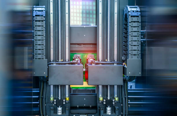
The process flow for flying probe testers generally involves the following steps:
- Setup: Set the tester and slide the PCB board inside the machine.
- Programming: Input the test specifications and PCB layout into the control system and the design of the electrical wire to deal with the parameters.
- Alignment: Take the use of cameras or any other alignment mechanisms to make sure that the probes exactly hit the points that have been allocated to the printed circuit board.
- Testing: Putting the probes into action by touching the test points will help to measure electrical properties of the PCB samples, such as resistance, capacitance, and continuity.
- Data Collection: Collect test data and report any deviation/failure from standard/expected.
- Analysis: Analyze the obtained information to pick up defective or defective parts of the PCB.
- Reporting: Create a detailed report highlight the test result and discuss any issues and provide feedback to be used to improve the performance of the institution.
- Adjustment: Adjust PCB design or production process if needed to incorporate what is observed in testing results.
Because of the simplified process used, the testing of PCBs is accurate and very deliberate, thus the production remains of high standard and there is reduced risk of errors.
FAQS
Here are some frequently asked questions (FAQs) about flying probe testing:
Conclusion
Whether you are looking for clues or secret information or information on how to create a living environment on another planet, these places have played a crucial role in avoiding or discovering the dangers of space. Leaving nothing to be desired in respect to the accuracy of the diagnostics and the cost to perform the testing, flying probe tests, the indispensable tool of the modern PCB manufacturers, is the answer to the puzzles facing the electronics industry. This technology of advanced testing is capable of not only increasing reliability of the manufactured products the manufacturers but also improve their production processes allowing for industrial innovation and quality improvement in electronics sector.

