Discover our deep insights on computer board testing. Learn the significance of the quality control process ensuring the low defect rate and high quality of the boards. Take enough time to learn extensively, including cases such as visual inspections up to the full functional test board kind. You would rather make the topic more important as your approach to industry regulations that deal with testing standards and describe the emerging technologies that are abrupt changers in PCB testing standards. Whether you are an expert or a beginner in this area of work, we have crafted our instructions in such a manner that it can offer useful tips about PCB testing.
What is PCB Testing?

PCB testing is an activity that consists on checking how the circuits specified in the printed circuit boards (PCBs) work, the quality of the circuits and their degree of reliability so as to guarantee that they conform to the pattern and performance. PCB testing is a necessary process in the electronics manufacturing industry every phase in order to identify whether there are defects, errors, or anomalies in the product that may hamper the functionality or durability the final product. Every stage of PCBs production is conducted through different testing methods and techniques that allow for the detection and fixing the errors at the time of production and before their application in electronics devices and manufacturing process.
Testing Methods for Printed Circuit Board
This Testing Methods makes sure that PCB manufacturers are in a position to meet quality standards, performance specifications, and reliability requirements, at the end of which they deliver reliable and top-notch electronic materials to customers. These are the overview of testing methods in burn in testing;
1. Visual Inspection in PCB Testing
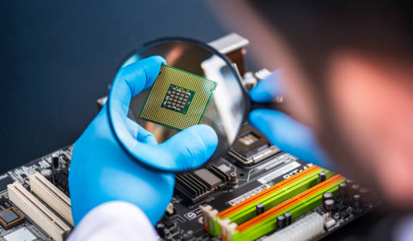
Visual inspection inherently can be considered one of the most basic and crucial types of PCB testing that involves practical evaluation and search of any PBC surface issues, while possible irregularities or anomalies can be looked through.
- Soldering Defects: Visual control is performed with the aim of identifying bridges, balls, insufficient solder, voids, or other solder defects. These errors may cause a bad contact, produce an open in circuit test, or give a short circuit and that’s why you’ll have a new PCB that cannot operate properly.
- Component Placement and Orientation: Visually inspecting and making sure that all the components are in the right place and properly oriented on the PCB according to the design specification is crucial. Deviating components or mismatching parts with wrong orientation can result in pcb assembly errors or mechanical difficulties.
- Component Damage or Physical Defects: Visual inspection goes hand-in-glove with checking for any signs of component damage, including but not limited to their cracked, chipped, bent and warped leads or broken connectors.
- Trace Damage or Copper Patterning Issues: The visual inspection verifies the circuit traces and decides whether there are any damages, such as scratches, breaks or any other problems.
- Conformity to Design Specifications: Visual inspection is used to ensure that the PCB matches the design specifications by verifying layer stack-up, component and trace routing placement, and solder mask alignment.
- Quality of Surface Finishes: Visual Inspection checks if surface finishes such as solder mask, silk screen pattern, and coatings (e.g., HASL, ENIG, and OSP) are up to standards. Any falls, failures or waviness in finishes’ surface will be detected and fixed to be one smooth and consistent one.
- Cosmetic Appearance: Visual Assessment Contributes to the Cosmetic Appraisal of the PCB Board Surface Condition, including Cleanliness, Uniformity of Markings, and Overall Visual Aesthetic Quality. While cosmetic flaws do not usually impact the right performance of the product, they can have serious implications concerning the quality of the final product from the point of view of a customer.
2. Manual vs Automated Optical Inspection
The decision to choose manual or automated inspection will depend on factors including the production volume, load capacity, budget limits, inspection needs, and the level of professionalism available. Up to this point, most companies combine these two techniques, though networking allows each method to play its role in creating robust PCB manufacturing.
Manual Inspection Advantages

Manual inspection present some principal purposes. The first advantage to be mentioned is that it offers the ability to adapt to different PCB designs and allows the operator to focus on the specific areas of interest in circuit testing, thus guaranteeing detailed inspection in line with each circuit board’s requirements.
Manual Inspection Disadvantages
Human observation, as much as we may cherish it, is not perfect. Primarily, it’s human error and subjectivity that’s at the core of the issue, as it is dependent on the skill and experience of human operators, who are the ones that may have variability and subjectivity in detecting defects. Additionally, human inspection is oddly slow against most automated systems, that results to longer inspection times, which can subsequently affect plant capacity.
3. Automated Optical Inspection (AOI) Advantages
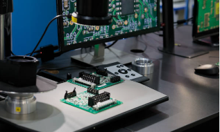
AOI machines come with their own bunch of merits relative to manual visual inspection done by human beings. First, they are able to inspect PCBs very fast, even much faster than the manual inspection method can so to a large extent, this instantly reduces inspection times and thereby increases production throughput.
Automated Optical Inspection (AOI) Disadvantages
AOI systems traditionally require a higher lump-sum payment to run the machines than manual inspection system do. This might not be a convenience for all manufacturers, as some may be on a budget, especially the small ones. Additionally, as should be expected in high-volume production, some flaws and anomalies may fall beneath the detection capabilities of AOI systems. These defects are typically more noticeable to a human operator with a good eye for detail.
4. X-Ray Inspection in PCB Testing
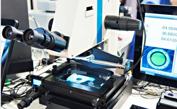
X-ray inspection is one of the non-destructive evaluation approaches that can be used to examine printed circuit boards for errors, anomalies, and embedded features that cannot be revealed through visual examination.
Principles of X-Ray Inspection
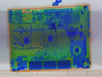
X-ray inspection makes use of X-rays, which are high-energy electromagnetic rays, to pass through materials and present the image based on the objects mass and a material it is made of. The PCB X-ray detects different tissues in the objects being radiated with X-rays by the absorption of the X-ray, such as copper traces, solder joints and components.
Applications of X-Ray Inspection in PCB Testing
X-ray inspection fulfills the role of detecting the defects and involvement in the solder joint verification, especially in the surface mount technology (SMT) components testing boards with hidden joints. Common applications of X-ray and inspection tool in PCB testing include:
- Solder Joint Inspection: X-rays can help detect soldering defects including but not limited to insufficient solder, cold solders joints, solder voids, solder bridging and tombstoning. It imparts piece of information with respect to quality and integrity of the solder joints, especially in the PCBs whose complexities are high and population is dense development.
- Component Alignment and Integrity: X-ray examination reveals the vertical and structural accuracy of hardware, comprising leaded and unleaded packages bundles, BGA (Ball Grid Arrays), CSP (Chip Scale Package) and QFN (Quad Flat No-Lead) elements. It maintains that parts are securely positioned; components are properly aligned and soldered to the PCB.
- Inner Layer Inspection: X-ray inspection is able to analyze the inner parts of the PCB which include the vias, traces, and inner layers through their electromagnetic radiation. It permits viewing inspectors to find faults which may include an open circuit or short circuit, blockage of debris, or delamination.
- Counterfeit Component Detection: X-ray inspection technique allows detection whether components are fake ones or have is hiding defects on an internal structure as well as on the packages or markings.
Advantages of X-Ray Inspection:
- Non-Destructive: X-ray inspection is a non-destructive method which enables inspectors to see inside the whole PCB without doing damage to the follow-up fluoroscopy analysis that contains detailed information about the internal structures of the PCB.
- High Resolution and Penetration: X-ray illumination systems have the ability to realize high resolution and penetrate through PCB materials, rendering visible internal structures and defects.
- Versatility: The X-ray method is very adaptive and could be applied for different types and sizes of PCBs, as well as various PCB assemblies such as multilayer boards, BGA components, fine-pitch components, and so on.
- Efficiency: X-ray inspection may be the fastest and can inspect many printed circuit boards or parts at the same time, that increases number of inspected pieces in a given time frame.
Limitations of X-Ray Inspection:
- Cost: X-ray inspection equipment is rather costly and requires ongoing support while it is used, necessitating expertise in its operation and the interpretation of the obtained results.
- Radiation Safety: X-ray checks do connect the operator to exposure of ionizing radiation; therefore, safety precautions and dealing with regulations should be taken.
- Complexity of Interpretation: Decoding radiographic pictures to discover faults may require specialized knowledge and experience, especially in cases with complex PCB operations and for complete defects.
In-Circuit Testing for PCB
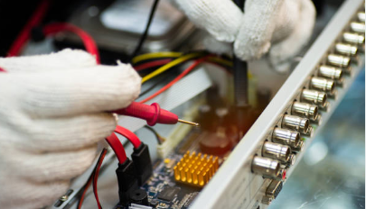
In-Circuit Testing (ICT) is an often-employed technique in the PCB manufacturing and assembly processes to help ensure that the electrical functionality and constituent parts of assembled PCBs are proper ict testing probes. Here’s an overview of In-Circuit Testing for pcb testing methods:
Principles of In-Circuit Testing
In-Circuit Testing utilizes individual components and trace testing on a pcb functional test circuit board with the whole assembly. The impedance matching network is in the form of a PCB, which is usually held on a specialized test fixture called a bed-of-nails fixture for which the contacts to the specific test points on the PCB are made.
Components of In-Circuit Testing
- Test Fixture: The test fixture is used to keep the PCB in position steadily and contains an array of hook-, knife- or tube-shaped test probes that are spring-loaded and meet the specified test point on the PCB. Pneumatics or hydraulics actuators may be included while provided for refusing rigorous interactions with the object.
- Test Probes: Test probes are pins or needles that are pushed against test points of the PCB and are spring-surrounded by the surrounding. The combination of both software and hardware components enables the successful execution of the test system signals and the reception of the PCB responses by the analyzing software.
- Test Instruments: The experimental equipment, including multimeters, oscilloscopes, and signal generators, are inserted to the PCB, among others, to get inputs, measure the parameters of electrical signals, and read the responses of the PCB.
Applications of In-Circuit Testing
In-Circuit Testing is test method used to test equipment and verify various aspects of PCB functionality and integrity, including:
- Component Testing: ICT ensures the appropriate position, alignment and functioning of each component, whether it be a passive component (resistors, capacitors) or active component (ICs, transistors), or connector.
- Interconnect Testing: ICT tells if there is the proper flow of current through traces, pads, and vias on the PCB or not. In ICT, the presence or absence of continuity, open or short circuits, is checked during the test process. It confirms order of signal paths, leading to the discovery of damages or discontinuities that may both be within the connections or communication links.
- Functional Testing: Besides testing single motion and cross-linking, ECT can check whether the prepared PCB operates the prescribed features and verify its functionality.
Advantages of In-Circuit Testing
- Comprehensive Testing: The ICT includes testing all single elements, their interconnections and the total system functionality. Such comprehensive evaluation is possible because ICT finds out whether the motherboard, the chip, whatever connects the motherboard and the chip actually work.
- High Accuracy: ICT provides a high degree of precision and accuracy in terminating negative phenomena through inspections like defects in the traces, open circuits, short circuits and particle solder problems in the PCB.
- Cost-Effective: In addition to the fast diagnosis of defects and issues via In-Circuit Testing (ICT), it is also cost-effective for medium- to high-volume production runs. This rapid ICT enables manufacturers to identify defects and issues at the start of the production process and avoid material and time waste during the manufacturing phase.
Limitations of In-Circuit Testing
- Limited Coverage: ICT might not be able to detect defects or issues in components that can not be understood in circuit, either because they are not visible, not testable, or because of the fine-pitch components made of hidden connections.
- Fixture Design: The design and production of custom test fixtures for ICT, especially for high-density PCB assemblies packed with components close together, would therefore require an enormous investment in time and money.
- Programming and Setup: The process of setting, programming and testing the ICT system for PCB designs involves skills, workmanship and time when test programs are to be developed and validated for each PCB design and assembly configuration.
Functional Testing for PCB
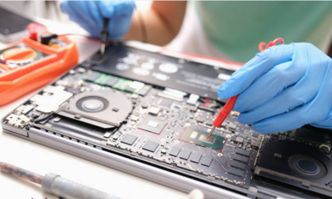
Functional tests for assembling the PCB consist of checking the overall operation of the PCB by applying input signals and analyzing output responses. Through this, it can be ensured that the PCB operates as specified in the design during functional testing.
Principles of Functional Testing
Functional stress tests are used to determine the ability of the PCB to work properly. They control the input wires on the device and see the results of applying exciting signals or experiencing thermal stress. It implies the implementation of the experiment via the process of mimicking the conditions typical for the PCB during the operation it would implement in its real-life application. Functional testing checks the circuit board’s potential to conduct signals, execute functionalities, and create the programmed reactions for the expected output response.
Components of Functional Testing
- Test Setup: The test setting includes the pertinent instruments and experimental equipment capable of both delivering input signals and measuring output responses, as well as evaluating the functionality of the board under the relevant test conditions.
- Test Procedures: Functional testing troubleshooting gives a structure that the particular tests, stimulus, and criteria which are used to check the correctness of the PCB. Here is the outline of the test conditions, which define the input, output response, pass/fail criteria, and special test parameters such as abnormal or emergency situations.
Applications of Functional Testing
Functional testing verifies various aspects to facilitate testing of PCB functionality and performance, and other functional tests include:
- Input/Output Verification: The functional testing confirms that, indeed, the circuit board is working up to the design specifications in that it reacts appropriately in response to the received signals and generates the intended output responses.
- Signal Processing and Conditioning: It evaluates the PCB’s aptitude to conditioning and processing signals, e.g. amplification, filterion, modulation, demodulation and signal encoding.
- Interface and Communication Testing: Communication interface testing validates the continuity and proper operation of interfaces that are important for data transfer, such as UART, SPI, I2C, Ethernet, USB or wireless communication settings, hence making data transmission and reception correct.
- Control and Logic Operations: It checks the running of control logic, microcontrollers, programmable logic devices (PLDs), and embedded firmware and software, confirming that the PCB performs functions similar to algorithms it is designed for.
Advantages of Functional Testing
- Comprehensive Assessment: Functional testing represents the primary type of testing which covers the overall performance and functionality of our board through an emulation of its future working environment and circumstances.
- Validation of System Integration: It verifies the integration and interaction of the components, subsystems, and interfaces on the PCB with the goal of confirming that the system functions according to the intended purpose in its target application.
- Identification of Design Issues: The functional testing may show us the design errors, code bugs or interfering performances which could be crucial during the PCB’s operation so that the problems can be fixed on -time before the deployment.
Limitations of Functional Testing
- Complexity: Functionality along with the testing can be as complex as the technicality of the test procedures, specialized equipments, and professionals with expertise in setting up and running the tests properly.
- Test Coverage: It may be difficult to get every test scenario and condition for each operating system, and the PCBs are highly integrated.
- Debugging and Troubleshooting: The time and resources needed for analyzing the results of testing and identifying the functional issues or failures may require additional time and resources, especially if these defects might be intermittent and hard to reproduce.
Simulating Real-world Conditions in Functional Testing

To ensure that real operating conditions, temperature cycles in case of mobile devices, device vibration, and other environmental factors are considered, running functional testing under such conditions is a safe environment, just like any real device would experience under operation and ball grid array packages. The operation of such procedure implies that the pertinent signals should be sent into the monitoring device. Further, various working conditions are supposed to be taken into account and some climatological factors such as vibration, mechanical forces, temperature and humidity should be incorporated. The simulation is carried out to verify the working of voltage (Vr), full range of load current (Iqr), and power quality (Pq). The transaction of information packages with different length and direction ties to PCB at the levels of interfaces facilitates the determination of the adaptiveness assumed by the card during the communications with the peripheral devices.
Importance of Quality Assurance in PCB Testing
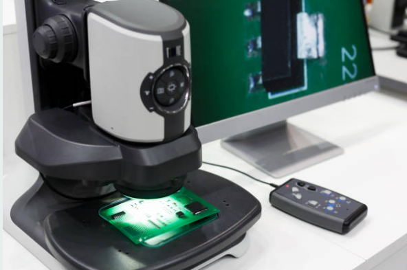
For feasible PCB quality fabrication, QA (quality assurance) is as essential as water, food and air are to humans. PCB QA prevents possible errors on boards, helps keep on record that the PCBs meet customer expectations, and ensures proven reliability of the PCBs. Here’s why quality assurance is crucial in PCB testing:
- Ensuring Product Quality: An automated QA procedure in PCB manufacturing will help to identify, fix, and correct issues, including bugs and defects, early. In this way, QA tries to provide quality and shield against incorrect or poor-quality products by taking very strict measures on details and standardizing product tests so no manufacturer can sell a faulty or substandard product.
- Compliance with Standards and Regulations: The standards which the International Organization for Standardization (ISO) imposes will ensure, from quality assurance perspective, that production of goods is efficient and safe enough, taking into account the functionality of regulations and the need of certification. By exacting the IPC standards, especially IPC-A-600 for product acceptability criteria (PCB), IPC-6012 for performance standards and ISO 9001 for quality management system, we signify that our PCB products are of optimal quality and worth trust, that helps us build a good reputation among customers and surrounding community.
- Minimizing Rework and Scrap: The QA testing work during PCB manufacturing identifies flaws earlier in the production process and, as a result, results in fewer reworks or throwaways.
- Enhancing Reliability and Longevity: PCB’s quality control programmed the board to meet the requirements of an uninterruptable condition and lifetime expected. A set of quality assurance procedures can be implemented at the location to verify that only pure parts are selected, welds are perfectly done and the intermediate connectors are error-free.
- Optimizing Production Processes: PCB QA methods provide superior method for optimizing manufacturing processes, increasing yield so that fewer faulty products are produced. First, QA examines the issue itself, including its causes and reasons. Following that, the QA takes measures and activities, and after each of them, it asks the organization to review the results.
- Protecting Brand Reputation: The reference to the steadiness and reliability of the PCB testing has the same importance for manufacturers who try to guarantee the brand image and product quality. Meeting the needs of the clients, PCBs are delivered with a strewing thing and combination of the acrostic checks are checked.
Certifications, Standards and Regulations in PCB Testing
In order to attain the certificates, standards, and regulations, those PCBs and electronic products shall be able to meet quality, safety, environmental, and regulatory requirements, which, in turn, will improve the performance, reliability, and market reception of the products.
- IPC Standards:
- IPC-A-600: Acceptability of Printed Boards This calls for the standards and acceptability criteria for bare PCBs, in other words, the seam tolerances, surface standards, and internal features, together with the relevant characteristics.
- IPC-6012: Specification for Inspection and Accurance Testing of Printed Boards: The document sets out the testing procedures and requirements for inspection and quality testing of rigid PCBs.
- IPC-610:Acceptability of Assembled PCBs: Creates acceptability standards for assembled boards, planning for items like soldering, component placements, and other quality attributes.
- IPC-J-STD-001: Soldered electrical and electronic joints and assemblies: Provides the requirements and acceptance criteria for soldered connections and assemblies, namely soldering processes, solder materials, and analyzing techniques.
- ISO Standards:
- ISO 9001: Quality Management System Requirements: Defines the requirements necessary to set up, keep up, maintain, and even improve quality management systems. Being issued the ISO 9001 certification certificate confirms that an organization has the capacity to always provide goods and services of acceptable quality that both the market and regulators require.
- ISO 13485: Medical Devices; Quality Management Systems; Requirements for Regulations: They establish quality management system requirements for organizations that are involved in medical device design, development, production, installation, and servicing.
- UL Certification:
- UL 94: Standard of Safety for Flammability of Plastic Materials for Parts in Devices and Appliances Testing sets fire testing methods and classification criteria for plastics, which devices and appliances are made of.
- UL 61010: Electricity Safety Rules for Equipment for Measurement, Control, and Laboratory: The rules for electrical safety that are adopted for device usage in measurement, control, and laboratory activities.
- CE Marking:
- CE Marking: Suggests conformity to the directives and rules of the European Union (EU), for example, security, Electromagnetic Compatibility (EMC), and environment directives. CE marking is the mandatory mark of trade agreement among the European Economic Area (EEA).
- RoHS Compliance:
- Restriction of Hazardous Substances (RoHS): The directive prohibits the use of certain harmful substances in the anatomy of electrical and electronic equipment. PCBs and electronic products fabricated according to RoHS standards are supposed to be devoid of materials of concern such as lead, mercury, cadmium and some of the first-generation flame retardants.
- REACH Compliance:
- Registration, Evaluation, Authorization, and Restriction of Chemicals (REACH): Regulation which concerns the chemical substances own production and application, which in turn have an impact on a person’s health and the ecological system. Compliance with the REACH Applies both polluting chemical compounds and stop orders related to chemical substances.
Makers will be expected to keep abreast of amendments being made to these standards and legislation in order to maintain conformity and the reputable quality and security of their product lines.
Challenges and Solutions in PCB Testing
PCB testing involves a number of problems because of the growing design complexity of electronics and also as a consequence of the expectation that they will last a long time and be of high quality. But the ever-inventive implementations of modern technologies have been a life saver in tackling these challenges exhaustively.
- Miniaturization and High Density: With electronic components getting smaller along the way, the PCBs are becoming more crowded and it is pretty difficult to access or test the components individually.
- Solution: During the process, the use of up-to-date testers like flying probe testing or boundary scanning brings in non-destructive testing of highly populated PCBs that do not need physical test points.
- Complexity of Designs: PCB designs are now evolving; they are getting more complex by the day, Artists are now are incorporating multi-layers, high-speed signal and mixed signal components to make testing a thorough comeback
- Solution: Modeling and simulation during the design phase utilize tools that can identify problems ahead of time. This allows the designers to redesign the layout to promote reliability testing. Also, the complex measurement techniques like signal integrity analysis and power integrity testing that manufacturer of high-speed circuits use guarantee stable performance.
- Variability in Components and Materials: The deviations in the component parameters and the PCB constructive materials tend to influence the testing results and the reliability of electronics.
- Solution: Using methods of statistical process control (SPC) and quality management systems technologies to provide constant monitoring and prevention of variation in PCB manufacturing is necessary to get 100% consistent and reliable results . Moreover, utilizing standard components and materials can improve process ability and component-to-component precision across batches.
- Time and Cost Constraints: Traditional testing methods include a long waiting time and high cost, which impede production efficiency and cost management.
- Solution: Introducing automated testing devices like automated optical inspection (AOI), in-circuit testing (ICT), or automated functional testing mechanics to the testing operation reduces the cycle time, minimizes the testing costs, and streamlines the whole testing process. There are other advantages to subcontracting testing services to special testing service providers, which is particularly useful for small and medium-sized manufacturers, which is an economic way.
- Environmental Testing Challenges: Environmental testing, which involves temperature cycling verification, humidity testing, vibration testing, and mechanical shock testing, should be provided to ensure PCB reliability in extreme operating environments.
- Solution: Allowing PCBs to undergo environmental tests in test chambers and equipment increases complete testing under various environmental conditions, making sure that PCB meets the requirements of reliability and durability. Secondly, ALT, or accelerated life testing, facilitates the reconstruction of failure modes and the robustness improvement of a product.
- Fault Diagnosis and Repair: Determining and diagnosing the defects of PCBs can turn out to be the most complicated task, especially when dealing with a complex infrastructure that has more than one element.
- Solution: Using advanced testing carriers like boundary scan testing, automatic fault-finding mechanisms, and built-in self-testing (BIST) techniques makes diagnostics better and provides a location for faulty components. Furthermore, thanks to the auto repair systems or reworking stations, the trend toward quick and precise state-of-the-art repairs for the detected faults will be developed.
Conclusion
To conclude, testing printed circuit boards (PCBs) is a decisive part of electronic manufacturing in order to guarantee the quality, reliability, and dependability of the electronic products. PCB inspection remains vulnerable to a number of complications, such as the small size of the PCB, the growing design intricacy, variable components, time- and cost-related constraints, environmental testing complexities, as well as fault diagnosis complexities. Although these new approaches break the traditional approaches, they solve those problems in an efficient way with new technological devices such as advanced testing technologies, automation, statistical process control, environmental testing equipment, and diagnostic algorithms. Through the adoption of thorough testing and evaluation schemes and procedural test methodologies, production problems can be solved and production efficiency can be increased, along with a decrease in costs and the achievement of better quality products and reliability. An increasingly advanced testing process further refines and optimizes the accuracy, performance, and manufacturing process of PCB testing as it aims to develop better and more reliable assemblies for different groups of users.

